
Nvidia is reportedly exploring the adoption of a multi-chiplet module (MCM) architecture for its forthcoming generation of GPUs, aligning itself with AMD and Intel in the pursuit of potential substantial performance improvements.
Traditionally, Nvidia has employed a single silicon slice for its top-tier graphics cards. However, recent rumors suggest that the company may make a significant shift towards a more versatile multi-chiplet module (MCM) design with its next-generation Nvidia Blackwell architecture.
The report, originating from renowned hardware leaker @kopite7kimi on X, indicates that Nvidia’s commercial-grade GB100 GPU could be the first to incorporate MCM technology.
The Nvidia Blackwell architecture is expected to underpin both Nvidia’s forthcoming commercial GPU products for data centers and industrial-scale users, as well as its consumer-focused Nvidia RTX 5000 series graphics cards.
While both product lines are anticipated to adopt the Blackwell architecture, it remains unclear whether the transition to MCM design will extend to the Nvidia 5000 series of consumer graphics cards. Should this transition occur, it could potentially deliver transformative performance enhancements to Nvidia’s next generation of graphics cards, addressing some of the performance limitations that have been evident in certain RTX 4000-series cards.
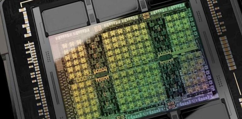
The MCM design, which combines multiple chiplets interconnected to function as a single processor, holds the promise of significantly boosted performance compared to traditional monolithic silicon chips. The physical constraints of silicon fabrication have limited the size of a single chip, with Nvidia already pushing the boundaries with its commercial-grade GPUs. Utilizing smaller chiplets and linking them with interconnects can effectively create a larger chip, offering the potential for substantial performance gains.
While these developments are still speculative and based on rumors, it’s worth noting that both AMD and Intel have adopted MCM designs in their GPUs and CPUs. Nvidia’s potential embrace of MCM technology reflects the industry’s response to the end of Moore’s Law, the historical prediction of doubling transistor density every two years. With transistors now approaching atomic size limits, alternative approaches, such as MCM design, are essential to deliver the expected performance improvements.
The prospect of distributing various GPU workloads, including geometry, rasterization, ray tracing, and machine learning, among specialized mini-processors within an MCM architecture presents an opportunity for faster and more efficient task execution. While the initial transition may not be as groundbreaking as the introduction of the first GPU over two decades ago, subsequent efforts are expected to yield significant advancements, positioning Nvidia competitively in the evolving landscape of graphics processing.