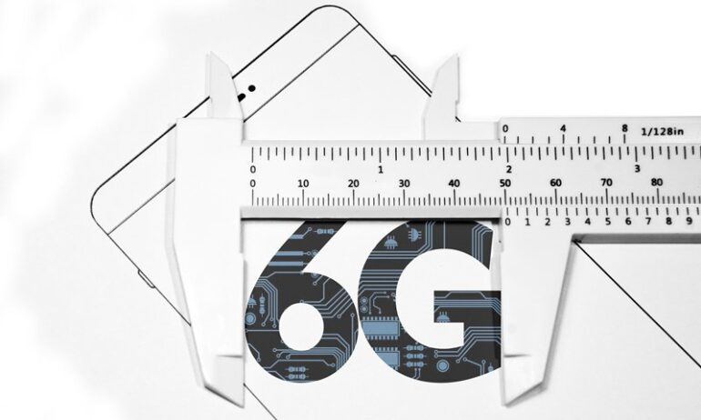

In the relentless pursuit of technological advancement, a team of researchers at Cornell University has taken a significant stride towards realizing the promise of 6G communication. Their groundbreaking work has yielded a semiconductor chip that could propel the minuscule devices of tomorrow into the high-frequency realms required for the next generation of wireless connectivity.
Table of Contents
Cornell Scientists Forge Path to Next-Gen Connectivity
As the world eagerly awaits the advent of 6G, one of the fundamental challenges lies in the need for greater bandwidth and higher frequencies. Traditional wireless communication devices, including the ubiquitous 5G smartphones, operate within the confines of frequencies below 6 gigahertz (GHz). However, the tantalizing prospects of 6G demand a bold leap into the uncharted territories of frequencies exceeding 20 GHz, where the allure of increased data throughput and unprecedented speeds lies.
The vision of 6G is nothing short of audacious – a promise of data rates a hundredfold faster than its 5G predecessor. Yet, as with any great technological leap, obstacles must be surmounted. In this instance, the very nature of high-frequency data transmission poses a formidable challenge, as the risk of signal degradation and data loss through environmental factors escalates with increasing frequencies.
Undeterred by these hurdles, the Cornell researchers have devised an ingenious solution – a complementary metal-oxide-semiconductor (CMOS) chip adorned with meticulously engineered 3D reflectors. These reflectors, intricately woven into a “tunable transmission line,” possess the remarkable ability to manipulate the time delay of signals across an astonishing bandwidth of 14 GHz, with a phase resolution of up to 1 degree.
Transcending the conventional approach of laterally spreading wavelength-long wires across the chip’s surface, the team envisioned a bold new paradigm – a three-dimensional realm where signals can be guided, reflected, and precisely timed. By winding the signal’s path through these intricate 3D waveguides and strategically bouncing signals off reflectors, the researchers have achieved a feat once thought improbable: packing an unprecedented number of delay elements into a minuscule area of just 0.13 square millimeters.
The implications of this innovation are profound. Traditional wireless arrays have long grappled with the trade-off between maintaining efficiency and shrinking their size to the scale of a chip. The Cornell team’s solution not only doubles the channel capacity – the very lifeblood of data rates – but also promises to bestow upon smartphone users a newfound bounty of data and unprecedented service speeds.
As Alyssa Apsel, a professor at Cornell Engineering and the senior author of the study, eloquently articulates, “The answer that most of the industry has landed on is, ‘Well, we can’t do time delay, so we’re going to do phase delay.’ And that fundamentally limits how much information you can transmit and receive.” Yet, their work suggests that a paradigm shift may be within reach, where a mere adjustment to a single component could ignite a tenfold increase in channel capacity, ushering in a revolutionary era of communication.
The details of this pioneering endeavor have been meticulously documented in the hallowed pages of Nature, a testament to the profound impact this research holds for the future of wireless connectivity. As the world stands poised on the precipice of a new technological frontier, the Cornell team’s achievement serves as a beacon of hope, illuminating the path towards a future where the boundaries of communication are pushed ever further, enabling unprecedented levels of connectivity and ushering in a new era of technological wonders.