
Nvidia revealed the successful fabrication of its first Blackwell wafer at TSMC’s state of the art facility in Phoenix Arizona. This milestone represents a pivotal advancement in bringing high performance AI chip production to United States soil reducing reliance on overseas manufacturing. The Blackwell architecture designed for next generation AI workloads promises up to 30 times the performance of previous generations enabling breakthroughs in data centers and computing applications. Nvidia’s commitment includes a planned investment of half a trillion dollars in AI infrastructure over the coming decade fostering innovation and job creation across the nation.
Blackwell Wafer Fabrication Process
The Blackwell wafer marks the initial output from TSMC’s advanced Fab 21 in Phoenix utilizing the 3 nanometer process node to produce chips with unprecedented density and efficiency. Each wafer can yield thousands of GPUs featuring the second generation Transformer Engine for enhanced AI inference and training capabilities. Production incorporates Nvidia’s proprietary design optimizations ensuring compatibility with CUDA software ecosystem for seamless developer integration.
Quality control measures at the facility include rigorous testing for defect rates below one part per million maintaining the high standards required for AI applications. The process is in line Nvidia’s recent goal of scaling output to meet global demand for Blackwell based systems in supercomputing and cloud services. This US based fabrication enhances supply chain resilience against geopolitical disruptions.
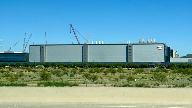
TSMC Phoenix Facility Overview
TSMC’s Phoenix plant represents a $65 billion investment in American semiconductor capacity with Phase 1 focusing on 4 nanometer and 5 nanometer processes before advancing to 3 nanometer for Blackwell. The facility spans 1 100 acres employing over 6 000 workers in roles from fabrication engineers to logistics specialists. It features cleanrooms exceeding 100 000 square feet equipped with cutting edge lithography tools and wafer inspection systems.
Energy efficient design includes water recycling systems reducing consumption by 40 percent and solar integration for sustainable operations. The plant’s location in Arizona leverages proximity to major tech hubs while benefiting from state incentives under the CHIPS Act. Full production ramp up is targeted for mid 2026 supporting not only Nvidia but future partners in AI and high performance computing.
The Half – Trillion Dollar NVIDIA masterplan
Nvidia’s ambitious plan allocates $500 billion over the next decade to expand AI capabilities through new data centers GPU development and ecosystem partnerships. This investment will fund construction of exascale supercomputers and edge computing solutions for industries including healthcare autonomous vehicles and scientific research. Key initiatives include collaborations with cloud providers like Microsoft Azure and Amazon Web Services to deploy Blackwell powered clusters. The strategy aims to create 100 000 high tech jobs in the US emphasizing training programs for semiconductor engineering and AI deployment. Funding will also support academic grants for university research in machine learning algorithms.
Blackwell GPUs deliver 20 petaflops of FP8 performance per chip with dual die configuration connected via NVLink for 1.8 terabytes per second bandwidth. The architecture introduces fifth generation Tensor Cores optimized for transformer models accelerating large language processing by five times over Hopper generation. Power efficiency improvements allow 70 billion transistors per GPU while consuming 30 percent less energy than competitors for equivalent workloads. Support for FP4 precision enables even faster inference in edge deployments like autonomous systems. The design incorporates advanced packaging with TSMC’s CoWoS L technology for higher interconnect density. These specifications make Blackwell suitable for training models with trillions of parameters pushing the boundaries of generative AI and scientific simulations.
Phase 2 of the Phoenix facility will add 2 nanometer capabilities by 2028 supporting next generation architectures beyond Blackwell with capacity for 20 000 wafers monthly. Nvidia plans to allocate 20 percent of Blackwell production to US fabs increasing to 50 percent by 2030. The company is also investing in advanced packaging facilities in Texas to complement wafer fabrication. International collaboration continues with TSMC’s Taiwan operations for volume production while US sites focus on high security applications. These steps ensure Nvidia meets projected demand for 1 million AI GPUs annually by 2027. The roadmap positions the US as a hub for AI hardware innovation.