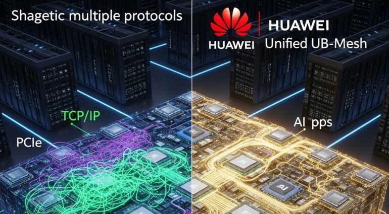

Huawei has announced its intention to open-source UB-Mesh, a new data center interconnect protocol designed to address scalability, performance, and cost challenges in large-scale artificial intelligence (AI) clusters. This move could have wide-reaching impact on AI data center infrastructure, potentially disrupting established standards such as PCIe, NVLink, CXL, and even conventional TCP/IP-based networking.
AI data centers that are now required to interconnect hundreds of thousands or even millions of processors, accelerators, memory modules, and storage drives, face increasing complexity and cost as they scale. Current industry practice relies on a mixture of protocols and standards (PCIe, NVLink, Ultra Ethernet, UALink, RoCE, TCP/IP) with each layer introducing conversion overhead, increasing power usage, and adding latency and potential failure points. For “gigawatt-class” AI data centers, the networking cost can rival the expense of the compute hardware itself.
Huawei introduced UB-Mesh at the Hot Chips 2025 conference as a unifying solution. UB-Mesh blends a high-capacity, CLOS-based backbone (an established scalable topology for data center switching) for hall-level coverage with a multi-dimensional mesh design within each rack or pod. This hybrid approach is intended to enable fine-grained, direct communications among nodes while enabling efficient scaling to tens of thousands of devices.
Now, let’s talk about the key features of the Huawei UB-Mesh
-
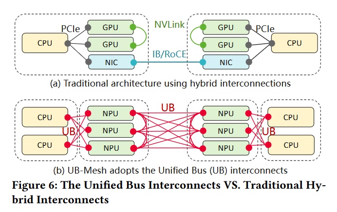
Unified Protocol: UB-Mesh aims to replace the current collection of interconnects with a single protocol. It allows any port (CPU, GPU, memory, SSD, NIC, switch) to connect with any other directly, eliminating the need for intermediary translation and reducing latency—targeting sub-microsecond (as low as 150 nanoseconds) intra-cluster communication.
-
Scalability: UB-Mesh is designed to support “SuperNodes,” Huawei’s term for ultra-large AI data center clusters operating as a single logical entity. Demonstrated in an 8,192-node deployment, it claims to flatten networking costs, avoid linearly scaling expenses, and integrate up to a million processors into a unified addressable system.
-
Optimized Topology: At the rack and pod level, UB-Mesh employs a n-dimensional full-mesh design to minimize reliance on expensive switches and optical modules, reducing infrastructural costs by up to 98% compared to traditional Clos-based fabrics for similar workloads. The protocol allows for modular expansion, flexible bandwidth allocation, and robust fault tolerance (such as maintaining communications despite component failures).
-
Performance: Huawei claims support for bandwidths above 1 terabyte per second per device, with synchronous load/store data semantics replacing traditional packet-based approaches. This is well beyond current PCIe 5.0 or even next-generation 8.0 standards, and is comparable to or surpasses plans for Ultra Ethernet and UALink, which have been developed as open industry consortium efforts.
-
Open Source Initiative: UB-Mesh will be published under a free license, with full technical details available at an upcoming Huawei conference. This is intended to encourage widespread collaboration and possibly establish UB-Mesh as an industry standard, subject to partner and customer adoption.
Questions remain about how UB-Mesh will coexist with legacy standards, integrate with existing hardware, and be governed over the long term in an open, multi-vendor environment. Being an open source project does not by itself address worries about proprietary control or long-term stewardship. While early demonstrations such as the 8,192-node “SuperNode” deployment are impressive, broader adoption will depend on independent validation, ecosystem support, and demonstration of cost and performance benefits at hyperscale operations.